


A lot of the technology that we rely on today we take for granted, but it’s hard to think about what the world would actually be like if we didn’t have access to these different pieces of tech. We rely on the likes of mobile phones, laptops, televisions, and computers every day, both in our personal and professional lives and as such, they now sit at the absolute foundation of our society. And at the foundation of these pieces of technology? It’s the PCB layout, without which a lot of these pieces of tech would not exist.
When it comes to actually creating a circuit board, the layout is the same as when an artist completes a piece of art. Engineers and electrical designers take plenty of time in putting together the perfect design that they are going to be able to use in the long run. If you are interested in putting together your own circuit board, then there are a number of different tips that you should be sure to keep in mind.
Contents
A lot of the below advice pertains to the actual design process involved in putting together a circuit board. They are very helpful throughout this whole process, but they’re not going to mean a lot if you don’t know where you should actually be sharing your designs once they are complete. There are a number of options, but one that is becoming more popular is using Altium and their compare Gerbers feature, which will allow you to put your Gerbers in front of people and see what the comments are on them. It’s an incredibly straightforward website to use and makes it easier than ever to put your completed designs in front of the right people and compare your work to see where you can improve.
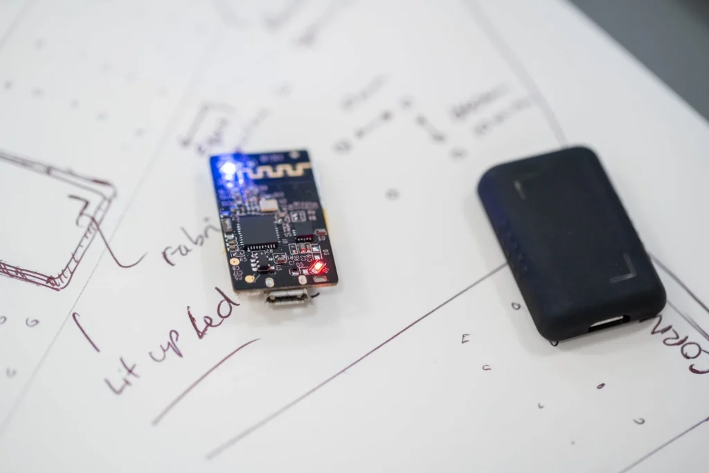
Have a Good Knowledge of the PCB Layout
A PCB layout specifically denotes the parts of the specific item, referencing how they are arranged and laid out. One of the most important aspects when it comes to the layout is the wire routing. A lot of experts believe that the design of the PCB tends to be about 90% placement and only 10% routing. The placement is where you will plan the different locations of various components, and the routing is where you add wires in order to connect various components based on different design rules.
There are two ways that the layout can be done, both manually and automatically. The majority of software which you will use for PCB design will have an auto-router feature, which saves time and makes the process simpler. That being said, this feature doesn’t always work, and a lot of designers, in this instance, will take more of a manual approach.
Ensure You Are Clear on Producer Demands
If you are about to begin designing, then it is vital that you have a clear understanding of producer demands. This means consulting your producer and ensuring you know exactly what they are looking at putting together. This means the number of layers that they are able to handle and other requirements which will be important in the design process too, like trace spacing and minimum trace widths.
Always Create a Ground Plane
When you are designing your PCB, it is important that you have a common ground terminal within the circuit schematic. This will provide different traces with the same reference point used for measuring voltages which is essential for your PCB layout. It’s not uncommon for different problems to arise when you start trying to utilize different traces rather than ground planes in order to route to the ground. There are three crucial roles that are played by the ground plane in PCB design, and these include the following:
- Voltage Return: Most (if not all) of the components that you would find within the PCB are connected to a power net. The ground net provides a pathway for the returning voltage.
- Signal Return: This is responsible for providing some kind of pathway that returns signals so that not too much interference is generated.
- Noise and Interference Reduction: When you create a ground plane’s huge conducting area, this is responsible for helping lower disturbance as it has a much lower impedance as opposed to when traces are used in order to route the ground net.
It’s important that you keep the above pieces of advice in mind whenever you design your PCB in order to make sure the process is as straightforward as possible, and your design at the end is efficient.